Power consumption is becoming an ever increasing problem in today’s laptops, cellular telephones, and portable music players.
This project will look at the effects of operating two simple 8 bit ripple carry adder designs at a very low sub threshold supply voltage. One design will be a static CMOS design, and one will be a dynamic CMOS design. The goal of this project is to deduce which method of construction will give the best performance while consuming the least amount of power. It is possible that the circuit may also consume the least power vs. speed of operation at a point not at the minimum supply voltage.
This adder could be used to control the access to music from either an optical disc or internal memory. This application will be used as the basis for the minimum operating characteristics. For a simple mp3 player the adder would need to address memory much like a program counter with a constant being added with the ability to jump. Most mp3 are encoded at 128kbps and 44.1 kHz. In the same way a CD player samples the data on the disc at 44.1 kHz, so if the simple adder where to be used in an audio device to control what would play (not decoding the signal) it must operate at least that speed, if not higher.
Project Floor Plan:
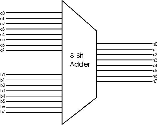
Figure 1. 8 Bit Adder
The two designs will both have the same topology, they will be 8 full single bit adders chained together. The total circuit will have 2-8 bit words as inputs, a carry in, a carry out. That makes for a total of 18 inputs. The circuit will output the sum and a carry out, for a total of 9 outputs.
The adder will be connected to a constant input and with a 2-to-1 Mux to give the ability for the circuit to select the previous sum, or jump to another input.
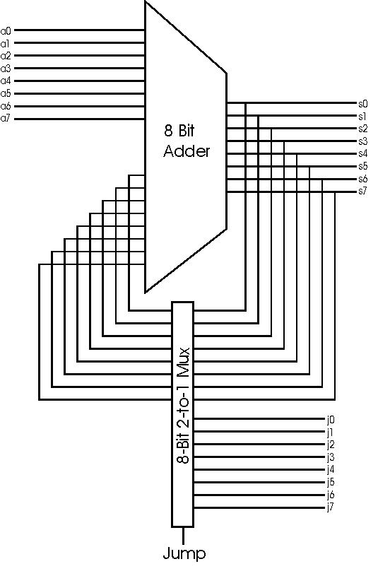
Figure 2. 8 Bit Adder With 2-to-1 Mux Allowing For Jump
The other project member is no longer enrolled in the class, so Andrew Cassell will be responsible for all design and testing.
(Top)Andrew Cassell
October 11, 2005
Subthreshold Data Path Circuit Design:
Two Implementations of Low Power Simple Adder
Project Specification:
For this project I will be doing two different implementations of a simple 8 bit program controller. The circuits will have the same topology, but one adder will be built using static CMOS construction, the other using dynamic CMOS construction. The circuit will be an 8 bit adder with one input connected to a static input of 00000001, the other input will be connected to a 2-to-1 flip-flopped Mux. The Mux will control whether the input to the adder will be the previous sum or a jump to value. This is designed to simulate the program control that would be required to continuously read from a memory address such as in a portable music player, but have the ability to skip(jump) to the next song in memory.
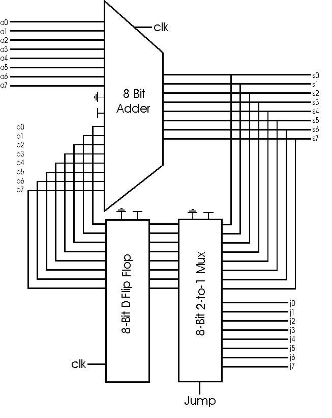
Figure 3. Circuit Topology: 8 Bit Adder With 2-to-1 Mux and D Flip Flop Allowing For Jump
The static versus dynamic circuits should be an interesting comparison. The static CMOS design will only dissipate dynamic(switching) power as there is no path from supply voltage to ground. However, the number of transistors in the static CMOS will be almost twice as many as the dynamic CMOS implementation. Static CMOS with a fan in of N requires 2N transistors. This may require more power to switch more transistors.
The dynamic CMOS will only require N+2 transistors for an input fan-in of N, which is substantially lower. The dynamic CMOS also consumes only dynamic power, however the overall power dissipation can be much higher. Finally the dynamic CMOS should be faster due to the reduced load capacitance attributed to the lower number of transistors per gate. Also the dynamic gates do not have short circuit current, and all the current provided by the pull-down transistors go towards discharging the load capacitance.
It will also require the clock, and possibly a skewed clock, be sent to every block in the circuit.
It may be possible that some sections of the design work best in static CMOS and some in dynamic CMOS. The circuit is going to be laid out in a modular form in MAX, so If testing of the components proves that some parts should be static, some dynamic, a third "uber" circuit will be constructed in the prototype phase and analyzed.
Block Specification:
8bit 2-to-1 Multiplexor:
This will allow us to select whether the input will be a jump or the previous sum to keep counting. It will be a basic 8 bit 2-to-1 Multiplexor Designed in Static and Dynamic CMOS respectively.
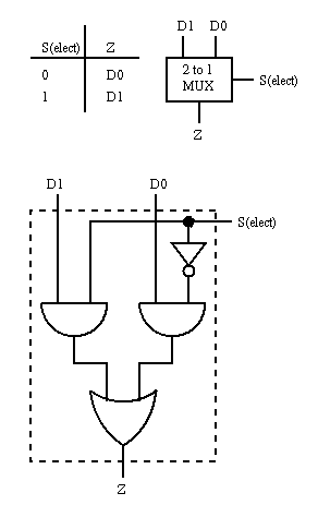
Figure 4. 2-to-1 Mux ( Choi)
D Flip Flop:
This block will keep the adder functioning at the speed of the clock, and keep the output from reaching the input before the next clock edge.
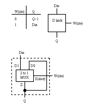
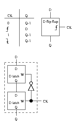
Figure 5. D Flip Flop(Choi)
8-Bit Full Adder:
I will using the ripple carry adder to try and reduce the number of transistors used, and based on the fact that the adder will be used much like a counter, not much carrying will have to propagate before the correct answer is achieved. The text suggests that if a more complex adder is used then the amount of power required to keep a desired performance could be lowered. However, in this experiment we will test only the advantages of dynamic vs. static implementations.
Because the inverting property of an adder:
S'(A,B,Cin)= S(A', B' Cin') and C'(A,B,Cin) = C(A', B', C') the inverters in the carry path become unnecessary.
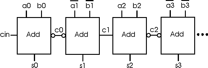
Figure 6. Full Adder Chain
For the static CMOS implementation a mirror adder will be used. The mirror adder is an improved design of the tradition full bit adder. It uses only 24 transistors and the those concerning the carry are placed closed to the output of the gate. Only the transistors in the carry stage of the circuit have to be optimized for speed. The most critical issue in the layout of the cell is the minimization of the capacitance at carry out.
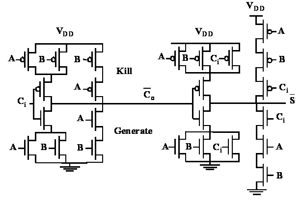
Figure 7. The Mirror Adder
For the dynamic design the mirror adder is stripped of it's pull up network and replaced with a clocked precharge transistor and an extra evaluation transistor on the pull down network.
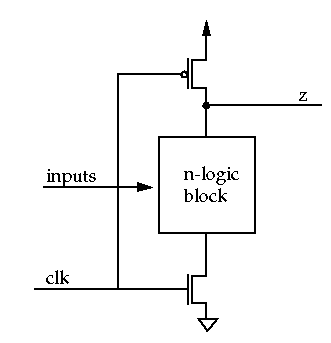
Figure 8. Basic Dynamic CMOS Design
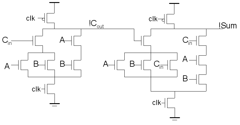
Figure 9. Dynamic CMOS Adder
Sources:
Paul GillardAndrew Cassell
November 15, 2005
Subthreshold Data Path Circuit Design:
Two Implementations of Low Power Simple Adder
Project Overview:
For this project I will be doing two different implementations of a simple 8 bit program controller. The circuits will have the same topology, but one adder will be built using static CMOS construction, the other using dynamic CMOS construction. The circuit will be an 8 bit adder with one input connected to a static input of 00000001, the other input will be connected to a 2-to-1 flip-flopped Mux. The Mux will control whether the input to the adder will be the previous sum or a jump to value. This is designed to simulate the program control that would be required to continuously read from a memory address such as in a portable music player, but have the ability to skip(jump) to the next song in memory.
1 Bit 2-to-1 Mux:
For the prototype I used a two stage NAND implementation of the Multiplexor.
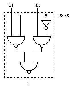
Figure 10. 1 Bit 2-to-1 Multiplexor (Choi)
Inputs and Outputs
Type |
Name |
Description |
|---|---|---|
Input |
D0 |
Data Input Selected When Sel goes Low |
Input |
D1 |
Data Input Selected When Sel goes High |
Input |
Sel |
Selects Which Data is Connected to Output |
Output |
Z |
Data Output |
Specifications
Measure |
Value |
|---|---|
Width |
6.8 |
Length |
17.37 |
Avg Power |
3.92μW |
Peak Power |
1.38mW |
Supply Voltage |
1V |
The Power supply rails extend on the left beyond the upper and lower bounds of the transistor layout to accommodate power rails. Inputs are taken from a metal layer.
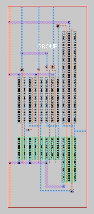
Figure 12. 2-to-1 Multiplexor VLSI Max Design
The block will receive a VDD of 1V during the final design to isolate the effects of the subthreshold testing to the add data path. Speed as a result should be no problem.
The following graph shows the 2-to-1 Multiplexor operating correctly, for all of the possible inputs. Not all of the possible transitions were considered, because this portion of the circuit should be much faster than the rest of the circuit as it will be operating above the threshold. The Z output follows the d0 input while the sel line is at 0, and then follows d1 when sel is at 1.
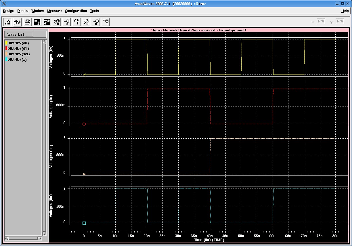
Figure 13. Awaves Output Plot of the 2-to-1 Mux
Files Related to the 2-to-1 Multiplexor:
| Description | Link |
|---|---|
| Max Layout | 2to1mux-cmos.max |
| HSpice | 2to1mux-cmos.sp |
| Inputs | 2to1mux-cmos.hsp |
| Measures | 2to1mux-cmos.mto |
1 Bit D-Flip-Flop
Using the design of the 2-to-1 Mux a D-latch was first constructed, and then used to create a positive edge triggered flip-flop.
Figure 14. D Flip Flop(Choi)
Inputs and Outputs
Type |
Name |
Description |
|---|---|---|
Input |
D |
Data Input |
Input |
Clock |
Triggers the Data to be read on rising edge |
Output |
Q |
Data Output |
Specifications
Measure |
Value |
|---|---|
Width |
14.85 |
Length |
17.40 |
Avg Power |
6.10μW |
Peak Power |
2.57mW |
Supply Voltage |
1V |
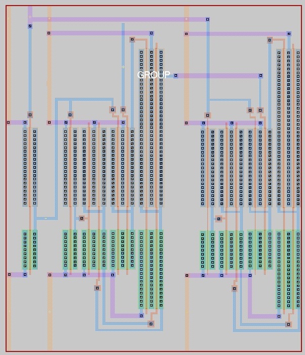
Figure 15. D Flip Flop VLSI Design
The block will receive a VDD of 1V during the final design to isolate the effects of the subthreshold testing to the add data path. Speed as a result should be no problem.
The following graph shows the D flip flop operating correctly, for all of the possible inputs. Not all of the possible transitions were considered, because this portion of the circuit should be much faster than the rest of the circuit as it will be operating above the threshold. The Q output follows the d input when the there is a rising clock edge.
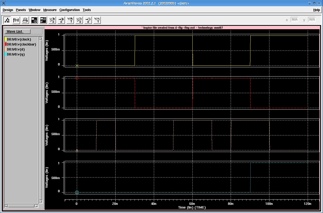
Figure 16. Awaves Output of the D Flip Flop Test
Files Related to the D Flip Flop:
| Description | Link |
|---|---|
| Max Layout | D-flip-flop.max |
| HSpice | D-flip-flop.sp |
| Inputs | D-flip-flop.hsp |
| Measures | D-flip-flop.mto |
Static CMOS 1 Bit Mirror Adder:
The prototype is a 1 bit full mirror adder designed in static CMOS.
.
Figure 17. The Mirror Adder
Inputs and Outputs
Type |
Name |
Description |
|---|---|---|
Input |
A |
Data Input |
Input |
B |
Data Input |
Input |
Cin |
Carry In |
Output |
Cout |
Carry Out |
Output |
Sum |
Sum |
Specifications
Measure |
Value |
|---|---|
Width |
10.69 |
Length |
21.16 |
Avg Power |
4.47μW |
Peak Power |
0.89mW |
Supply Voltage |
1V |
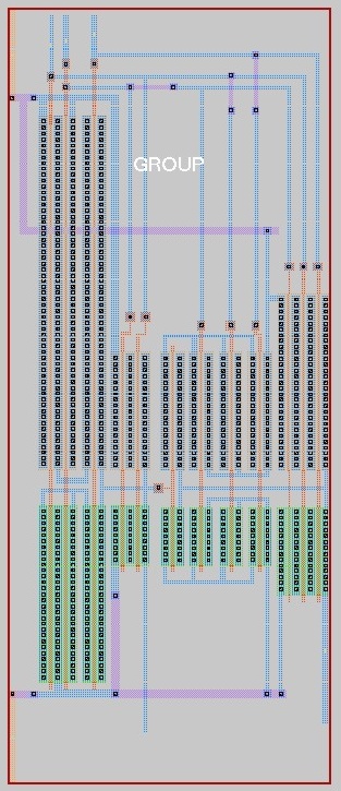
Figure 18. The Mirror Adder VLSI Design
The following graph shows the cmos adder operating correctly, for all of the possible inputs at a supply voltage of 1V. Speed was not considered because the design is going to focus on achieving to lowest power which the greatest speed for an operating block of 8 units.
Note: Cin and Sum in the plot are actually Cin' and Sum'
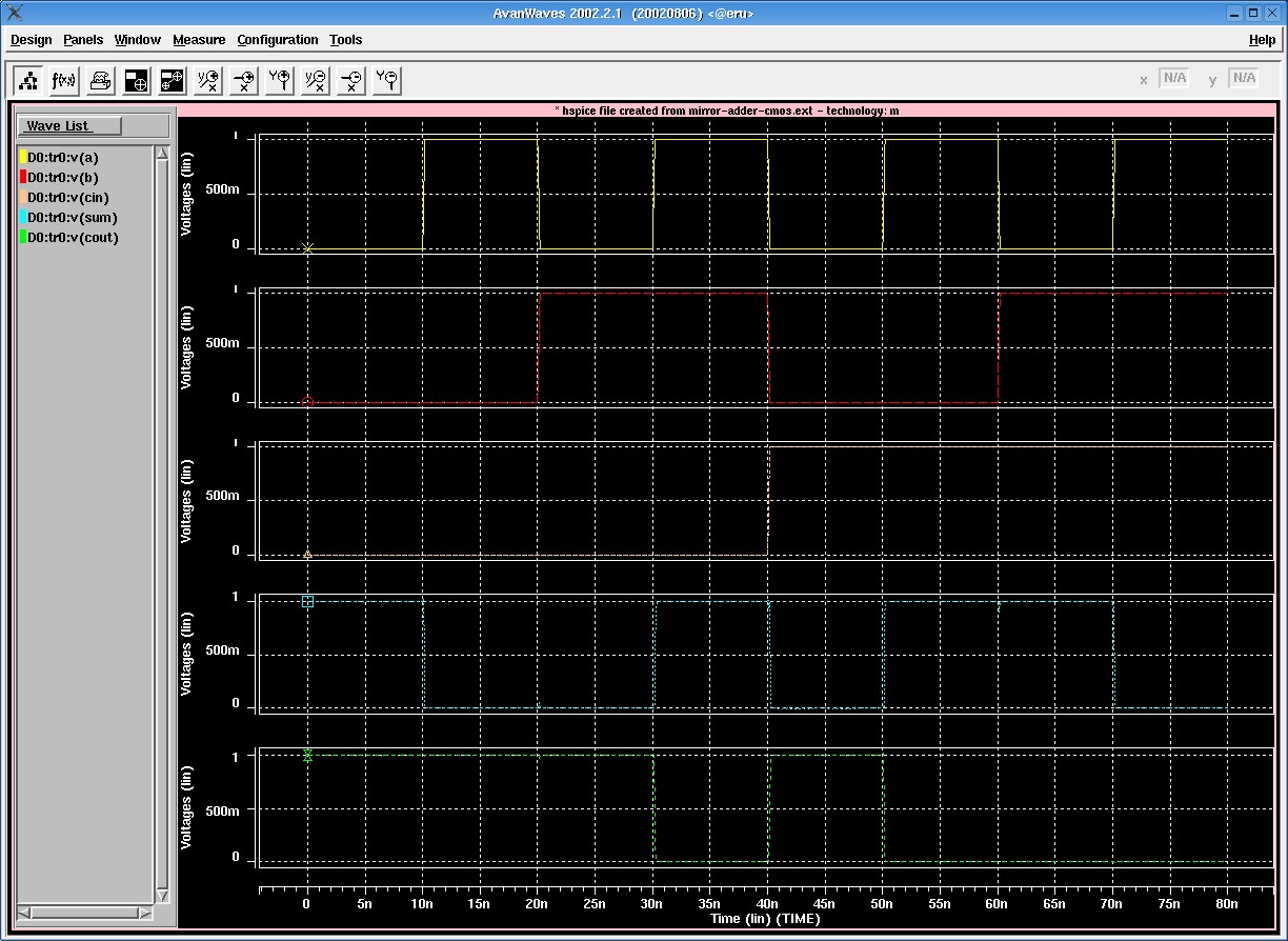
Figure 19. Awaves Output Test Waveform
Files Related to the D Flip Flop:
| Description | Link |
|---|---|
| Max Layout | mirror-adder-cmos.max |
| HSpice | mirror-adder-cmos.sp |
| Inputs | mirror-adder-cmos.hsp |
| Measures | mirror-adder-cmos.mto |
Dynamic CMOS 1 Bit Mirror Adder:
The prototype is a 1 bit full mirror adder designed in dynamic CMOS.
.
Figure 20. The Dynamic Mirror Adder
Inputs and Outputs
Type |
Name |
Description |
|---|---|---|
Input |
A |
Data Input |
Input |
B |
Data Input |
Input |
Cin |
Carry In |
Input |
Clock |
Clock Signal |
Output |
Cout |
Carry Out |
Output |
Sum |
Sum |
Specifications
Measure |
Value |
|---|---|
Width |
13.9 |
Length |
23.19 |
Avg Power |
5.94μW |
Peak Power |
1.53mW |
Supply Voltage |
1V |
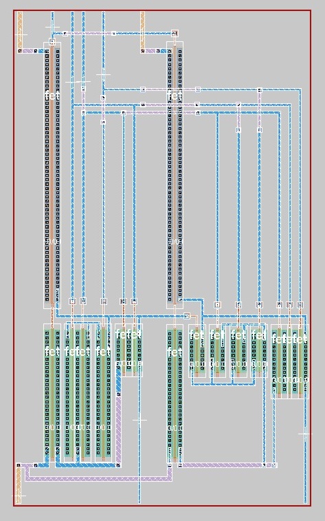
Figure 21. The Dynamic Mirror Adder VLSI Design
The following graph shows the dynamic adder operating correctly, for all of the possible inputs at a supply voltage of 1V. Speed was not considered because the design is going to focus on achieving to lowest power which the greatest speed for an operating block of 8 units.
Note: Cin and Sum in the plot are actually Cin' and Sum
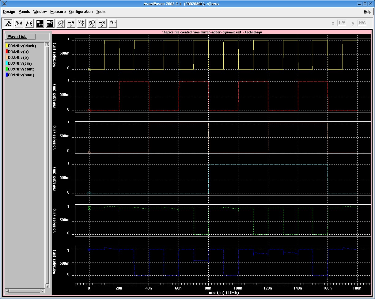
Figure 22. Awaves Output Test Waveform
Files Related to the D Flip Flop:
| Description | Link |
|---|---|
| Max Layout | mirror-adder-dynamic.max |
| HSpice | mirror-adder-dynamic.sp |
| Inputs | mirror-adder-dynamic.hsp |
| Measures | mirror-adder-dynamic.mto |
Comparison
So far the CMOS design appears to consume the least amount of power. To design this part of a music player, most power use is going to come from the dynamic power. As a result I expect to see the CMOS's dynamic power to be less, but the dynamic circuit should use less static power.
Andrew Cassell
December 5, 2005
Subthreshold Data Path Circuit Design:
Two Implementations of Low Power Simple Adder
Project Overview:
For this project I will be doing two different implementations of a simple 8 bit program controller. The circuits will have the same topology, but one adder will be built using static CMOS construction, the other using dynamic CMOS construction. The circuit will be an 8 bit adder with one input connected to a static input of 00000001, the other input will be connected to a 2-to-1 flip-flopped Mux. The Mux will control whether the input to the adder will be the previous sum or a jump to value. This is designed to simulate the program control that would be required to continuously read from a memory address such as in a portable music player, but have the ability to skip(jump) to the next song in memory. The design however failed to perform as expected.
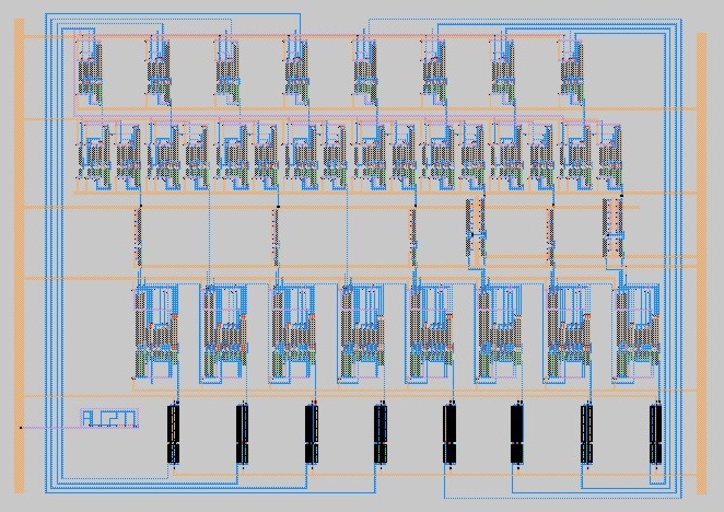
Figure 22. Static CMOS Layout
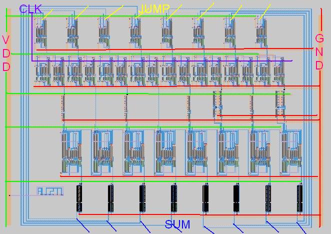
Figure 23. Static CMOS Layout With I/Os Labeled
The design was 159.100 X 111.730, but was plauged with problems. The counter never quite functioned correctly with the flip flops in place. The system had inputs for VDD, GND, clock, JUMP input, and a 8 bit input for Jump Address. The counter does count to about 4 and then loses it self once the carryout is passed.
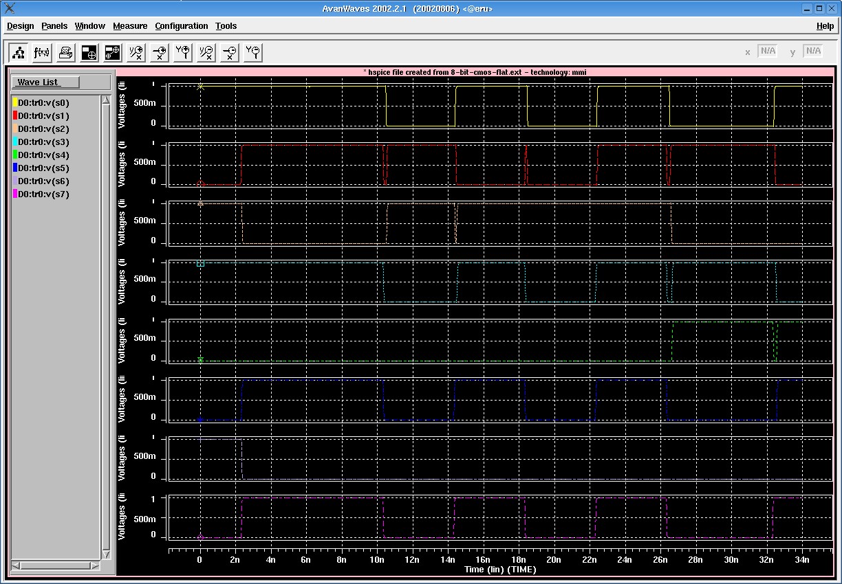
Figure 24. Static CMOS Awaves Output
The layouts were optimized by making sure each component fit nearly the same form factor when placed on the grid. This allowed the GND and VDD lines to be easily placed going horizontally in an evenly spaced out manner. By using a cascading adder design, in which the carry's are not put through an inverter between each adder, I was able to reduce the area needed. The transistors were sized to the proper size for the mirror adders to insure optimum performance and to balance the upswing and downswing charactaristics.
Conclusions
To make a comparision between the dynamic and static CMOS designs as the correspond to power usage, I will examine the single bitter adders when they are not connected to the rest of the system. The static CMOS design uses less dynamic power, and because the counter is switching constantly very little static power will be dissipated. As you can see in the graph below, there are biggest reductions in the power consuption when we use sub threshold design. You can see the change in the curve as the VDD approaches Vt.
Supply (V) |
Static CMOS Avg (W) |
Static CMOS Max (W) |
Static CMOS RMS (W) |
Dynamic CMOS Avg (W) |
Dynamic CMOS Max (W) |
State CMOS RMS (W) |
1.0 |
2.62E-06 |
1.23E-03 |
3.25E-05 |
5.94E-06 |
1.50E-03 |
6.48E-05 |
0.8 |
1.33E-06 |
5.64E-04 |
1.56E-05 |
2.70E-06 |
6.10E-04 |
2.81E-05 |
0.6 |
6.89E-07 |
2.57E-04 |
7.33E-06 |
1.34E-06 |
2.97E-04 |
1.24E-05 |
0.4 |
3.25E-07 |
9.84E-05 |
2.66E-06 |
6.24E-07 |
1.05E-04 |
4.30E-06 |
0.3 |
1.85E-07 |
2.50E-05 |
9.82E-07 |
3.69E-07 |
4.27E-05 |
1.80E-06 |
0.2 |
8.21E-08 |
3.22E-06 |
2.05E-07 |
1.59E-07 |
3.94E-06 |
3.72E-07 |
0.1 |
1.19E-08 |
2.06E-07 |
1.78E-08 |
1.78E-08 |
1.98E-07 |
2.29E-08 |
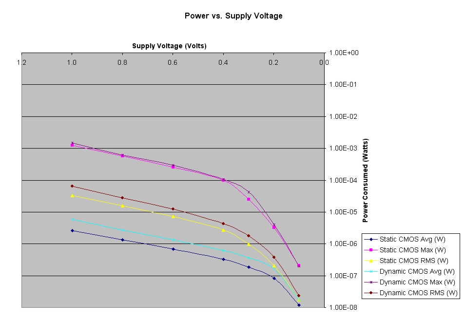
Figure 25. Power Comparison
Here are the two circuits operating at below threshold:
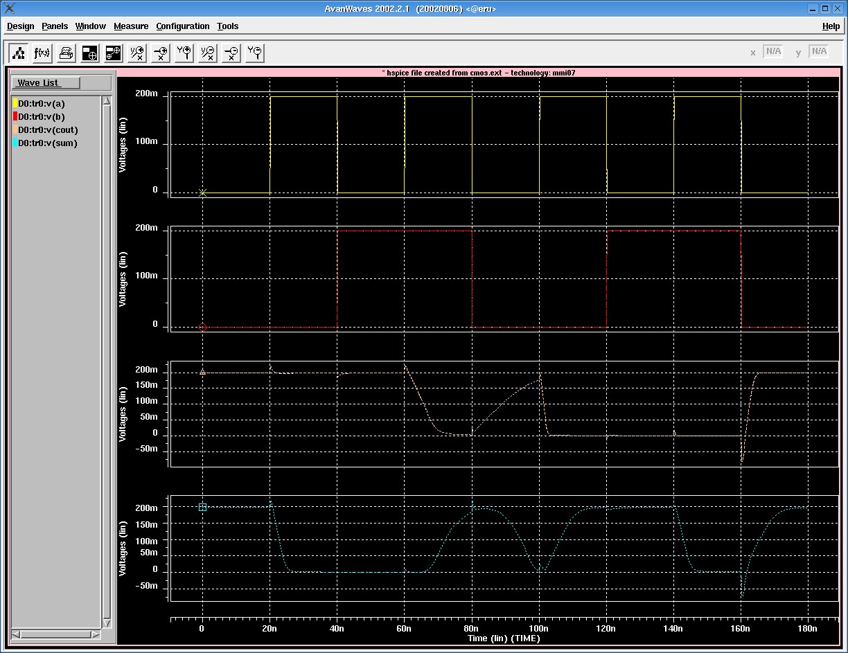
Figure 26. Static CMOS at .02V VDD
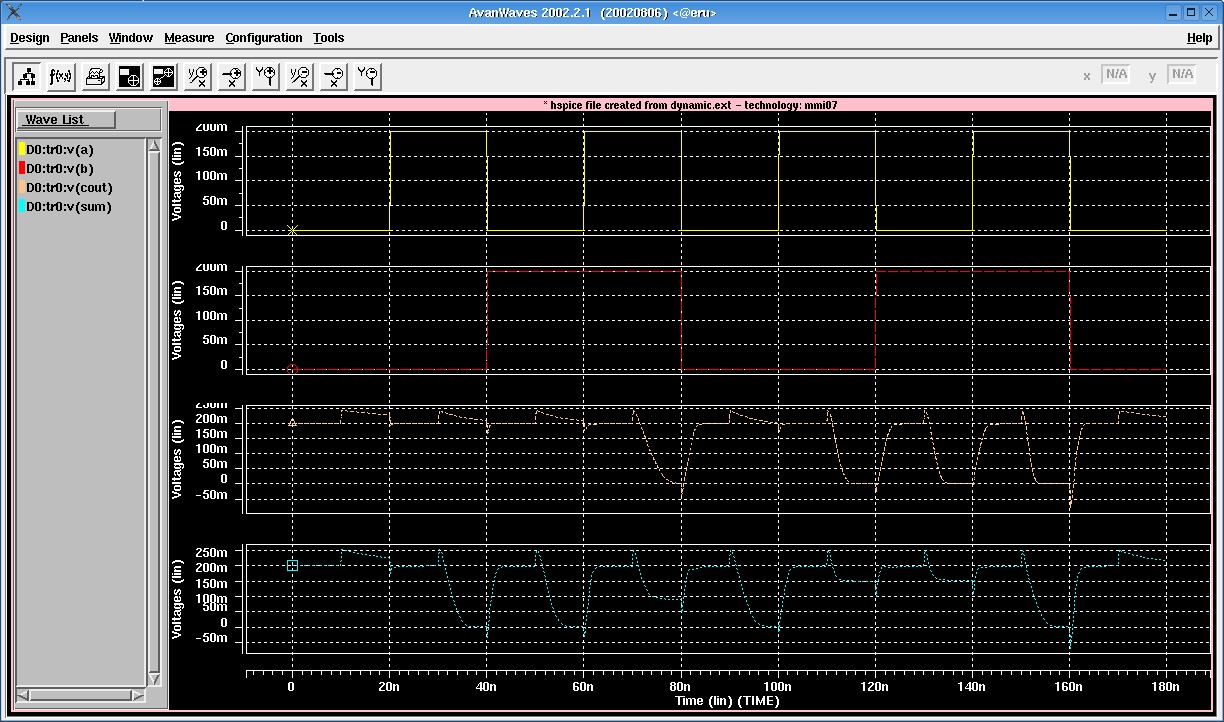
Figure 25. Dynamic CMOS at .02V VDD